Inside the platform
Define the requirements
What does the device need to do? Set the operating conditions and manufacturing constraints before choosing a material.
See a full record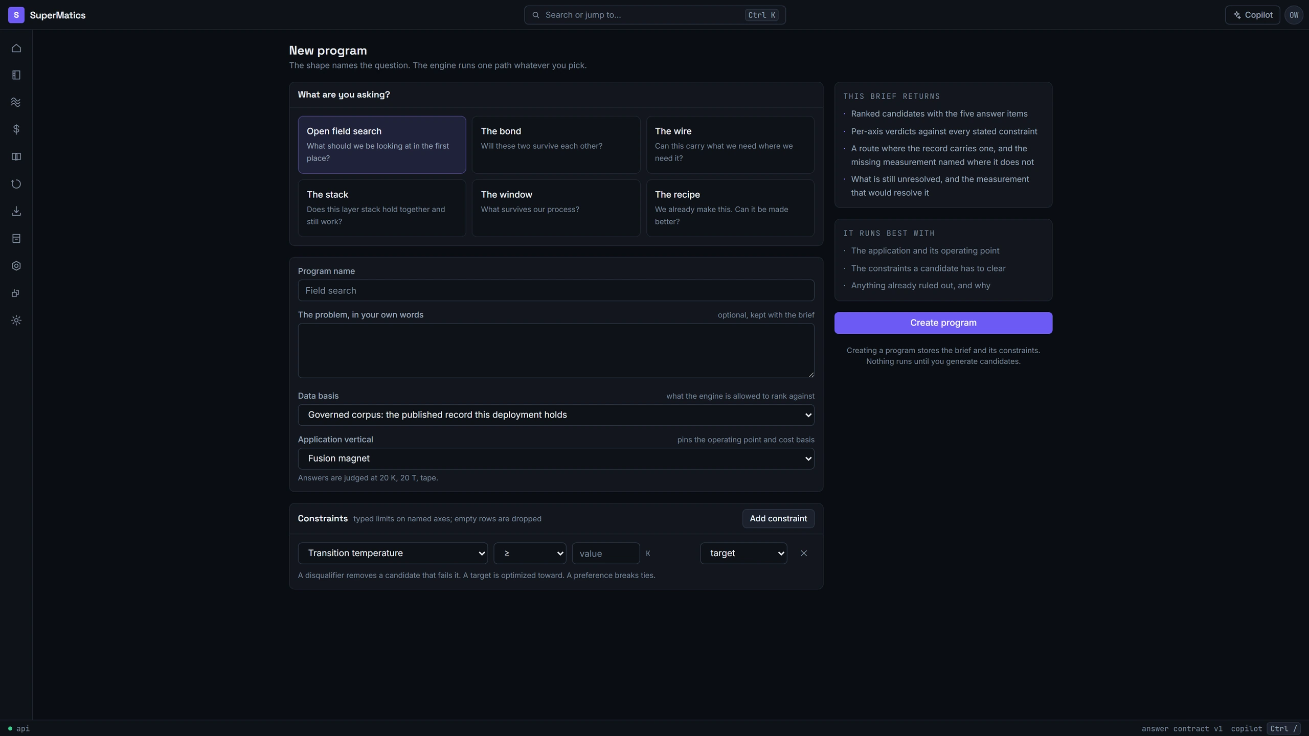
Superconductor R&D
SuperMatics finds the materials and manufacturing processes your device needs, then makes and measures them: lab work at Berkeley, partner benches, and pilot runs with manufacturers.

Inside SuperMatics
Inside the platform
What does the device need to do? Set the operating conditions and manufacturing constraints before choosing a material.
See a full recordInside the platform
Compare materials, their interfaces, and the processes that make them. See which requirements each option meets, what the evidence supports, and where the gaps remain.
See a full record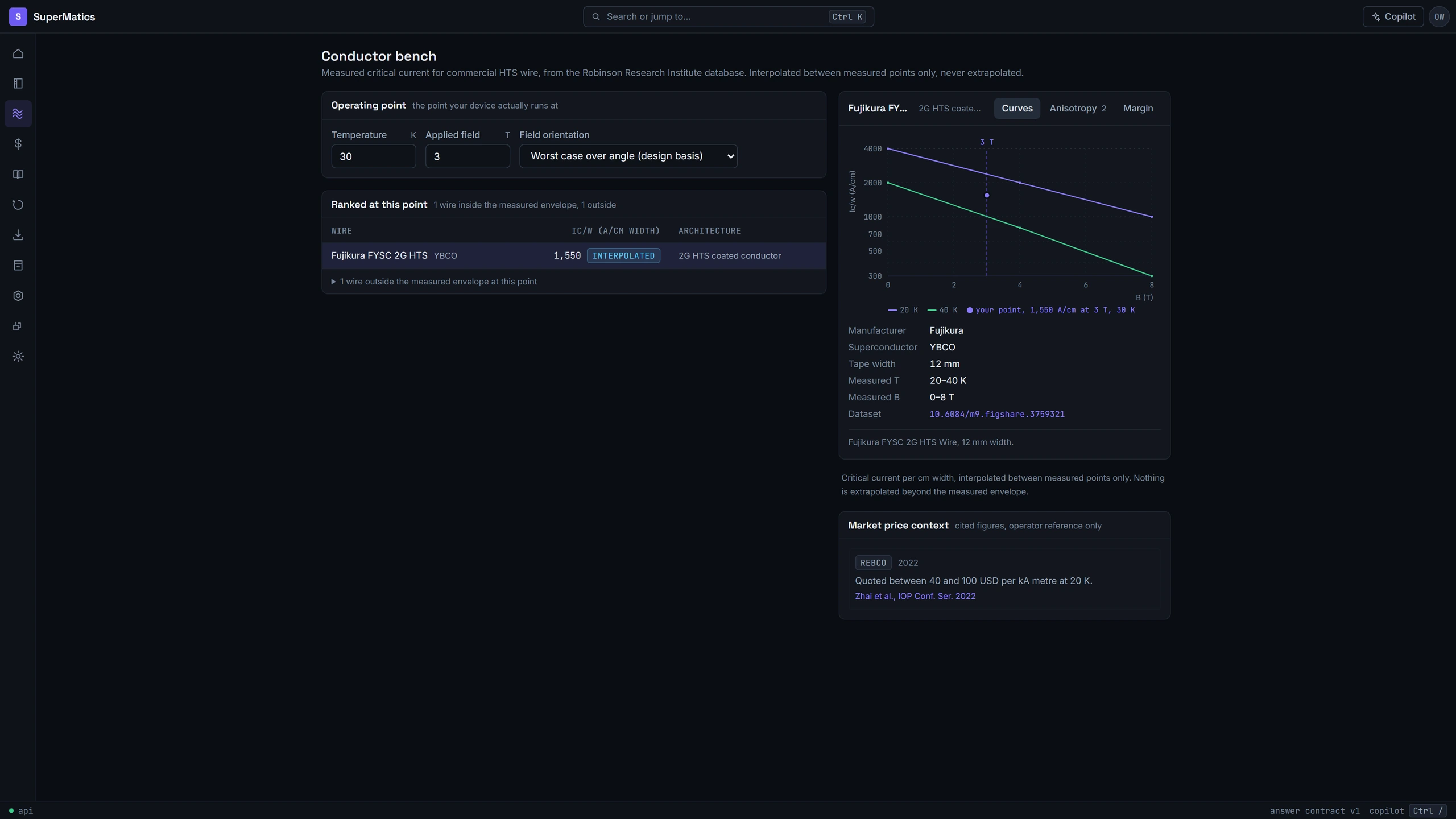
Inside the platform
Agree on what to build and measure. Search and ranking run in weeks; lab work follows partner calendars. Synthesis is moving in-house at Berkeley. Every result informs your next decision and the model.
See a full record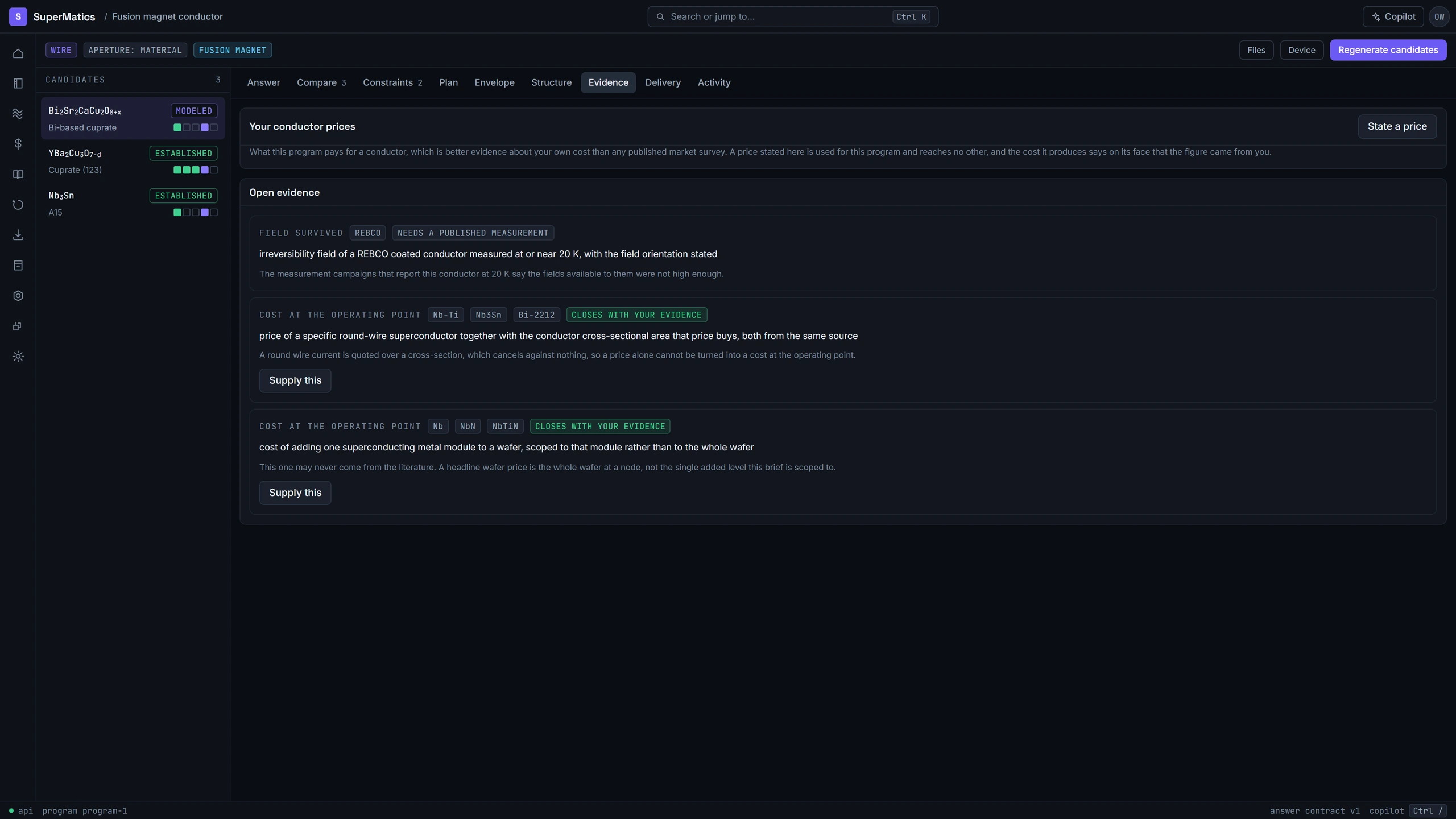
Representative software views. Explore the worked cable example on Platform.
The network behind SuperMatics
Customer & synthesis partner
Live with CAN Superconductors today. Paid search campaigns are running with fusion and quantum hardware teams.
An exclusive framework license from Hyunsung TNC. 20+ patents, issued and pending.
Explore the networkBrookhaven · Walther-Meissner-Institut
Single-crystal growth and characterization.
UC Berkeley QB3 · CAN Superconductors · Eloi Materials
Deposition, etching, precursor powders and industrial synthesis.
Georgia Tech · UIUC
Scanning tunneling microscopy and spectroscopy.
An effect consistent with a central MEL prediction was measured independently at Stanford and SLAC, with no involvement from us.
Lee et al. · Phys. Rev. Lett. 2026 ↗Working together
Our business combines platform software licenses, paid development programs, and licensing of materials and processes we own.
Talk to us about your projectCustomer-operated access is planned. Our team runs it and reviews every record today.
Paid programs address your device requirements, from the search to a measured sample and a pilot run.
Our discovery research pursues materials and processes we could license.

Our own search
Alongside our customer work, we search for new superconductors. Every result informs the next search.
Explore discovery